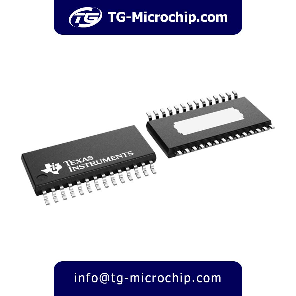
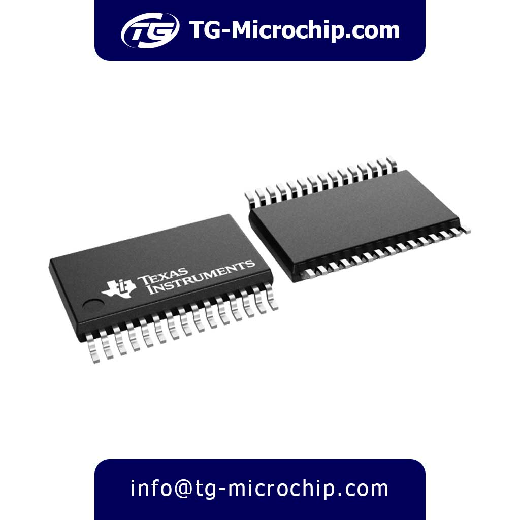
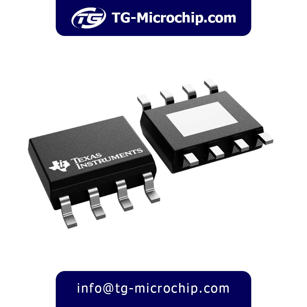
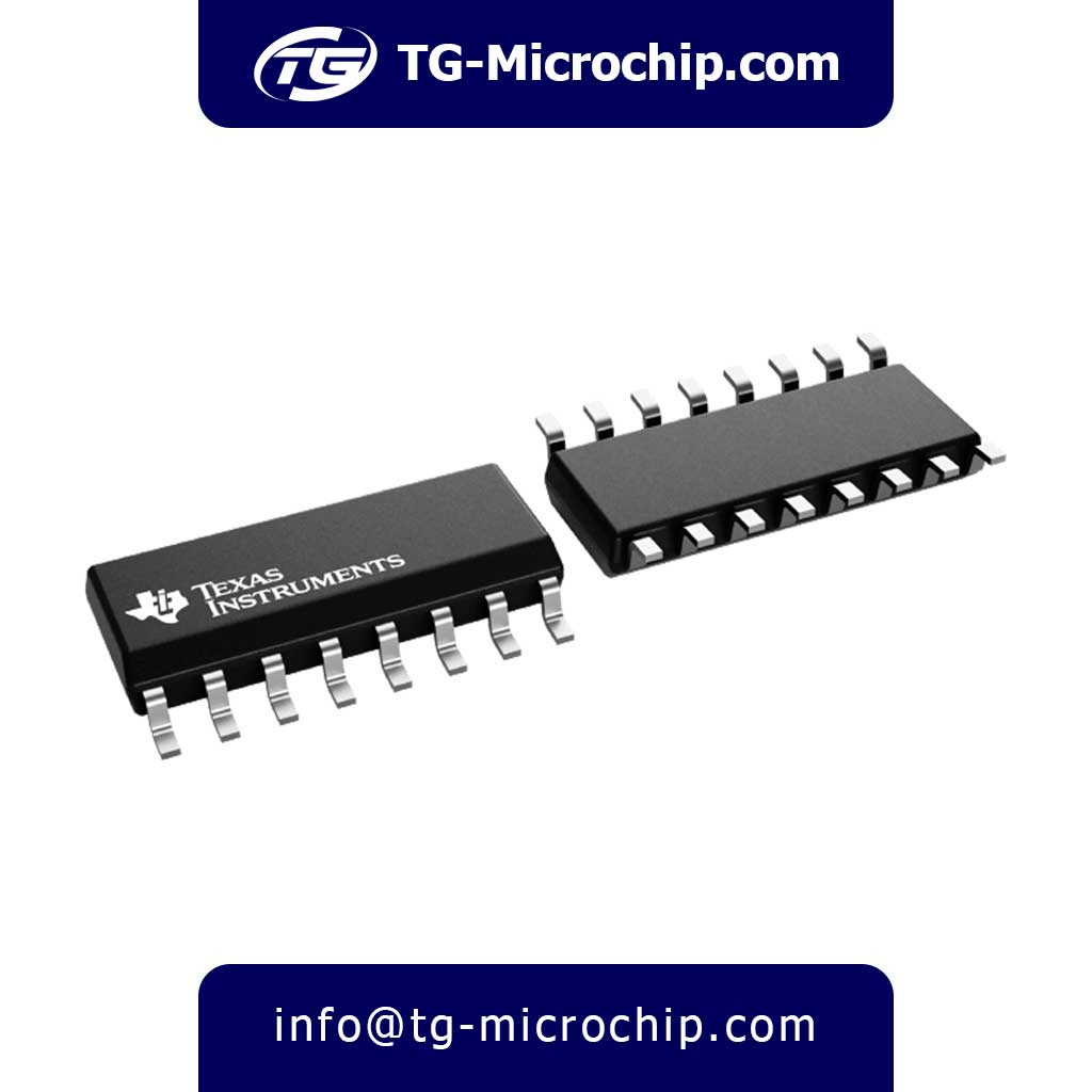
For order or price inquiry of TMUX6219DGKRQ1 Texas Instruments Please click on Buy Order button and fill the RFQ form we will check out inventory and offer you our best price.
Quick Access
About
The TMUX6219DGKRQ1 from Texas Instruments is a high-performance, automotive-grade analog switch designed for precision signal routing applications. This single-pole double-throw (SPDT) switch features an ultra-low on-resistance of just 2.5Ω (typical) and supports a wide voltage range from 5V to 36V (single supply) or ±5V to ±18V (dual supply). Its break-before-make (BBM) switching action prevents signal shorts during transitions, making it ideal for sensitive measurement systems. As an AEC-Q100 Grade 1 qualified device, it meets stringent automotive reliability requirements for operation from -40°C to +125°C.
With an impressive 200MHz bandwidth and minimal charge injection (1.5pC), the TMUX6219DGKRQ1 delivers excellent signal integrity for high-speed analog and digital signals. The switch exhibits low distortion (0.01% THD+N) and high off-isolation (-60dB), ensuring clean signal transmission in audio, video, and data acquisition systems. Its rail-to-rail signal handling capability and 1.8V/5V logic compatibility make it versatile for interfacing with modern microcontrollers and sensors. These characteristics position it as an ideal solution for test equipment, battery management systems (BMS), and automotive electronic control units (ECUs).
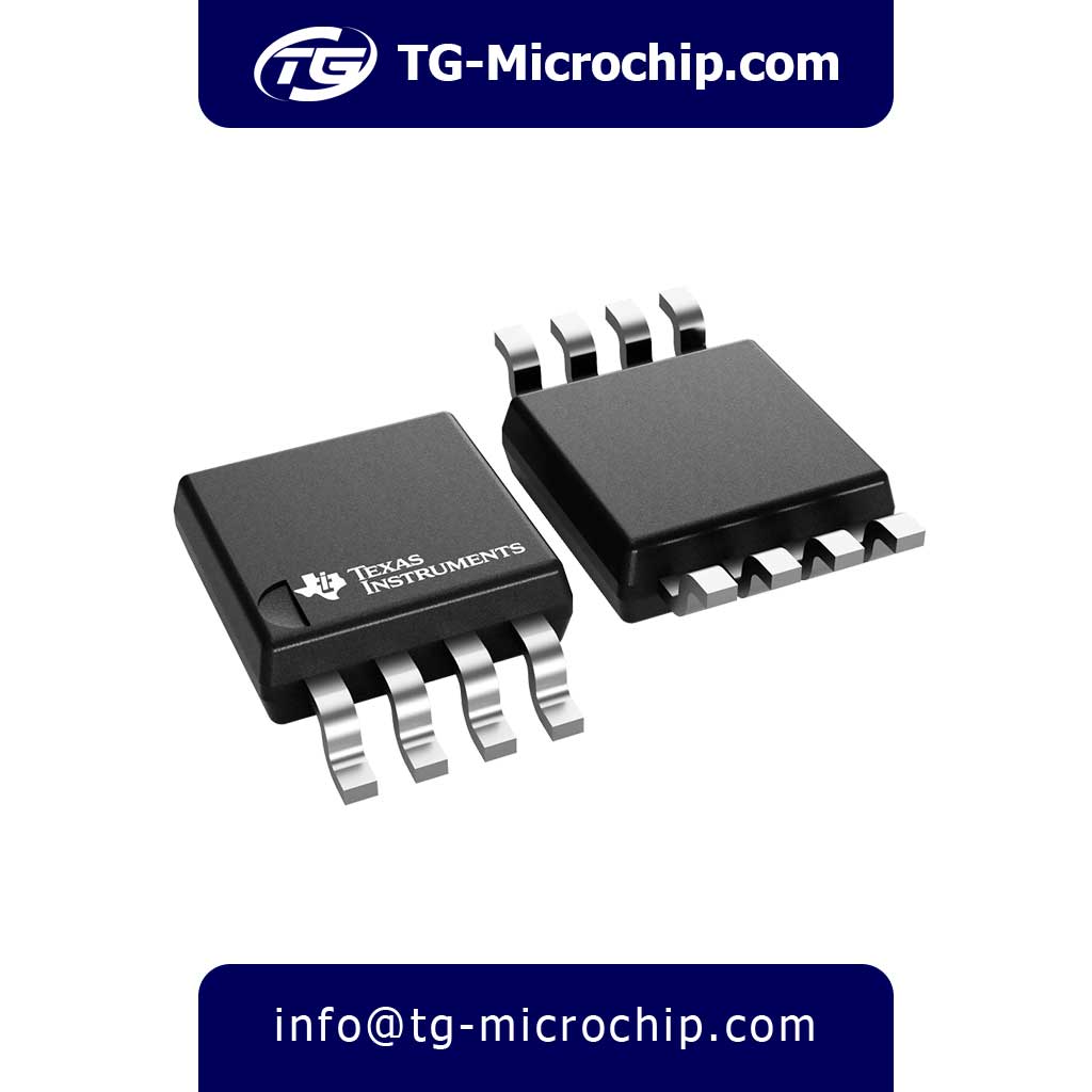
Packaged in a space-saving VSSOP-8 (3mm × 3mm) format, the device is optimized for compact PCB designs while maintaining robust performance. The surface-mount package supports automated assembly processes and is supplied in tape-and-reel packaging for high-volume production. With ±2kV ESD protection (HBM) and a moisture sensitivity level (MSL) rating of 1, it withstands harsh manufacturing and operational environments. These mechanical and reliability features make it particularly suitable for automotive and industrial applications where durability is critical.
Texas Instruments provides comprehensive support for the TMUX6219DGKRQ1, including SPICE models for simulation and PPAP documentation for automotive customers. The combination of electrical performance, rugged packaging, and automotive qualification makes this analog switch a reliable choice for mission-critical systems. Whether used in vehicle infotainment, ADAS sensors, or industrial automation, it offers a robust solution for precision signal routing. Its balanced mix of speed, accuracy, and reliability addresses the growing demands of next-generation electronic systems.
Features
High-Performance Signal Switching
- SPDT Configuration (Single-Pole Double-Throw)
- Ultra-Low On-Resistance (RON): 2.5Ω (typical) @ 5V supply
- Low RON Flatness: 0.5Ω (typical) for consistent signal integrity
- Wide Analog Signal Range: Supports rail-to-rail switching
2. Broad Power Supply Flexibility
- Single-Supply Operation: 5V to 36V
- Dual-Supply Operation: ±5V to ±18V
- 1.8V/5V Logic-Compatible Control Inputs (TTL/CMOS)
3. Superior Signal Integrity
- High Bandwidth: 200MHz (-3dB) for high-frequency signals
- Low Charge Injection: 1.5pC (typical) (minimizes glitches)
- Low Distortion: 0.01% THD+N (@ 1kHz, ideal for audio)
- Excellent Isolation:
- Off-Isolation: -60dB (@ 1MHz)
- Crosstalk Rejection: -80dB (@ 1MHz)
4. Automotive-Grade Reliability
- AEC-Q100 Qualified (Grade 1) for harsh environments
- Extended Temp Range: -40°C to +125°C
- Robust ESD Protection: ±2kV HBM (JESD22-A114)
- PPAP Support Available for automotive customers
5. Compact & Robust Packaging
- VSSOP-8 (3mm × 3mm) Package – Space-efficient for dense PCB layouts
- Tape & Reel (3000 units) for automated assembly
- MSL Level-1 Rated (Moisture-resistant, 260°C reflow capable)
6. Fast & Reliable Switching
- Break-Before-Make (BBM) Action – Prevents signal shorts
- Fast Switching Times:
- Turn-On (tON): 50ns (typical)
- Turn-Off (tOFF): 30ns (typical)
7. Precision Analog Switching Performance
- Low On-Resistance (RON):
- 2.5Ω (typ) at 5V | 3.5Ω (max) across temperature
- Near-Zero RON Drift: <0.1Ω/°C variation (-40°C to +125°C)
- Break-Before-Make (BBM) Switching:
- Guaranteed dead time >5ns between channel transitions to prevent shoot-through.
- Charge Injection: 1.5pC (typ) at 5V, critical for:
- Sample-and-hold circuits
- Precision ADC/DAC interfaces
8. Power Supply & Efficiency
- Single/Dual-Supply Flexibility:
- Single-Supply: 5V to 36V (e.g., 12V automotive bus compatible)
- Dual-Supply: ±5V to ±18V (for bipolar signal handling)
- Low Quiescent Current: 1µA (max) in standby mode (V+ = 12V)
- Power-Off Protection:
- Signal pins remain high-impedance when unpowered (0V to 36V tolerant).
9. High-Fidelity Signal Handling
- 200MHz Bandwidth (-3dB):
- Maintains signal integrity for:
- Video routing (HDMI/LVDS buffers)
- RF front-end switching (up to VHF range)
- Maintains signal integrity for:
- THD+N Performance:
- 0.01% (typ) @ 1kHz (10kΩ load) – Suitable for:
- Automotive audio systems
- Medical instrumentation
- 0.01% (typ) @ 1kHz (10kΩ load) – Suitable for:
- Off-Isolation & Crosstalk:
- -60dB @ 1MHz (channel-to-channel)
- -80dB @ 1MHz (adjacent signal rejection)
10. Automotive & Industrial Robustness
- AEC-Q100 Grade 1 Certified:
- Validated for:
- 1000+ temperature cycles (-40°C ↔ +125°C)
- 85°C/85% RH humidity bias testing
- Validated for:
- Enhanced ESD Protection:
- ±2kV HBM (all pins)
- ±1kV CDM (JESD22-C101)
- Latch-Up Immunity:
- Exceeds 100mA per JESD78D.
11. Timing & Control Features
- Propagation Delay: 15ns (typ) for logic control signals.
- Logic Thresholds:
- 1.8V CMOS-compatible (VIL = 0.5V, VIH = 1.3V @ 1.8V supply)
- 5V TTL-compatible (VIL = 0.8V, VIH = 2V @ 5V supply).
12. Mechanical & Packaging
- VSSOP-8 (DGK) Package:
- 3.0mm × 3.0mm footprint – 50% smaller than SOIC-8.
- 0.65mm pin pitch – Compatible with fine-pitch PCB designs.
- Green Packaging:
- Halogen-free (IPC/JEDEC J-STD-709 compliant).
13. Application-Specific Optimizations
- Battery Management Systems (BMS):
- Low RON minimizes voltage drop in cell-balancing circuits.
- Automotive Sensors:
- EMI-hardened design for CAN/LIN bus signal routing.
- Test & Measurement:
- <1nA leakage ensures accuracy in µV-level measurements.
14. Design & Support Tools
- SPICE Model Available – Simulate switching transients in LTspice/PSpice.
- Evaluation Module (EVM): TMUX6219EVM for rapid prototyping.
Specifications
| Parameter | Specification | Notes |
|---|---|---|
| Basic Information | ||
| Manufacturer | Texas Instruments | – |
| Part Number | TMUX6219DGKRQ1 | – |
| Product Category | Analog Switches & Multiplexers | – |
| Product Type | Precision SPDT Analog Switch | Break-Before-Make (BBM) |
| Description | 1-Channel SPDT, Low RON, Wide Voltage Range | AEC-Q100 Qualified |
| Electrical Characteristics | ||
| Supply Voltage (Single) | 5V to 36V | V+ to GND |
| Supply Voltage (Dual) | ±5V to ±18V | V+ to V- |
| On-Resistance (RON) | 2.5Ω (typ), 3.5Ω (max) | @ V+ = 5V |
| RON Flatness | 0.5Ω (typ) | – |
| Bandwidth (-3dB) | 200MHz (typ) | @ V+ = 12V, RL = 50Ω |
| Charge Injection | 1.5pC (typ) | CL = 1nF |
| Off-Leakage Current | 1nA (max) | @ 25°C |
| Turn-On Time (tON) | 50ns (typ) | RL = 50Ω, CL = 5pF |
| Turn-Off Time (tOFF) | 30ns (typ) | – |
| Logic High (VIH) | 2V (min) | @ V+ = 5V |
| Logic Low (VIL) | 0.8V (max) | @ V+ = 5V |
| ESD Protection | ±2kV HBM | JESD22-A114 |
| Mechanical Specifications | ||
| Package Type | VSSOP-8 (DGK) | – |
| Dimensions | 3.0mm × 3.0mm | Body size |
| Pin Pitch | 0.65mm | – |
| Mounting Type | Surface Mount | SMD |
| Packaging | Tape & Reel | 3000 units |
| MSL Rating | Level-1 | 260°C reflow |
| Environmental & Reliability | ||
| Operating Temp | -40°C to +125°C | Automotive Grade 1 |
| Storage Temp | -65°C to +150°C | – |
| AEC-Q100 | Grade 1 Qualified | Full testing |
| MTBF | >1M hours | Estimated |
| RoHS Compliance | Yes | Lead/Halogen-Free |
| Signal Performance | ||
| Signal Range | Rail-to-Rail | – |
| THD+N | 0.01% (typ) | @ 1kHz, RL=10kΩ |
| Crosstalk | -80dB (typ) | @ 1MHz |
| Off-Isolation | -60dB (typ) | @ 1MHz |
| Applications | Automotive ECUs, BMS, Test Equipment, Data Acquisition | – |
| PPAP Capability | Yes | For automotive |
Advantages
1. Unmatched Signal Integrity
- Ultra-Low 2.5Ω On-Resistance
- Minimizes voltage drop and distortion in high-precision circuits (e.g., sensor interfaces, ADC front-ends).
- 5× lower RON than standard analog switches (e.g., typical 10Ω–20Ω switches).
- 200MHz Bandwidth
- Maintains signal fidelity for high-speed data/video routing (e.g., automotive cameras, RF test equipment).
- Near-Zero Distortion
- 0.01% THD+N (1kHz) for clean audio/power measurements.
2. Automotive-Grade Reliability
- AEC-Q100 Grade 1 Certified
- Operates reliably in -40°C to +125°C environments (vs. commercial-grade 0°C to 70°C).
- Validated for 1000+ thermal cycles and humidity bias tests.
- Robust ESD Protection
- ±2kV HBM (all pins) protects against electrostatic discharge in harsh environments.
- Latch-Up Immune
- Exceeds 100mA per JESD78D (critical for 12V/24V automotive systems).
3. Power Efficiency & Flexibility
- Wide Supply Range
- 5V to 36V (single supply) or ±5V to ±18V (dual supply) – Supports legacy and modern systems.
- 1µA Quiescent Current
- Ideal for battery-powered or always-on applications (e.g., IoT, BMS).
- Power-Off Protection
- Signals remain isolated when unpowered (0V–36V tolerant).
4. Space-Saving & Manufacturing-Ready
- Compact VSSOP-8 Package (3mm × 3mm)
- Saves 50% board space vs. SOIC-8 – Critical for dense automotive/industrial PCBs.
- Tape-and-Reel (3000 units)
- Enables automated pick-and-place assembly.
- MSL Level-1 Rated
- Withstands 260°C reflow soldering without baking.
5. Application-Specific Benefits
- Automotive ECUs
- Low RON reduces error in throttle position sensors or fuel injector controls.
- Battery Management (BMS)
- <1nA leakage prevents cell imbalance in multi-cell Li-ion packs.
- Test & Measurement
- 1.5pC charge injection avoids false triggers in precision sampling.
6. Design Support & Longevity
- SPICE Models Available
- Simulate switching behavior in LTspice/PSpice before prototyping.
- PPAP Documentation
- Streamlines compliance for automotive OEMs.
- Texas Instruments’ Supply Chain
- Guaranteed long-term availability for industrial/automotive programs.
Applications
1. Automotive Systems
- ECU Signal Routing – Switches sensor signals (throttle, pressure, temperature) in engine control units.
- Battery Management (BMS) – Cell voltage monitoring and balancing in EV/HEV batteries (low RON minimizes voltage drop).
- Infotainment & ADAS –
- Audio signal switching (0.01% THD+N for clean output).
- Camera/video signal routing (200MHz bandwidth for LVDS/HDMI).
- CAN/LIN Bus Isolation – Protects communication lines from transient noise.
2. Test & Measurement Equipment
- Data Acquisition (DAQ) – Multiplexes low-voltage analog signals (<1nA leakage ensures accuracy).
- Automated Test Systems (ATE) – High-speed channel switching (50ns transition time).
- Oscilloscope Probes – Signal path selection with minimal distortion.
3. Industrial & Automation
- PLC I/O Modules – Isolates analog inputs (e.g., 4–20mA sensors).
- Process Control – Switches thermocouple/RTD signals in temperature monitoring.
- Motor Drive Systems – Routes feedback signals (encoder, current sense) with low RON.
4. Medical Electronics
- Patient Monitoring – ECG/EEG signal routing (high off-isolation prevents crosstalk).
- Diagnostic Equipment – Precision switching for blood glucose/pH sensors.
5. Consumer & Communication
- Audio Systems – Selects between inputs (DAC, mic) with near-zero distortion.
- RF Front-Ends – Antenna switching (200MHz supports VHF/UHF bands).
6. Aerospace & Defense
- Avionics – Reliable signal routing in flight control systems (–40°C to +125°C operation).
- Telemetry – Multiplexes sensor data in harsh environments.
Comparison with Similar Components
| Parameter | TMUX6219DGKRQ1 (TI) | ADG1419 (Analog Devices) | MAX14752 (Maxim) | TS5A23159 (TI) |
|---|---|---|---|---|
| Configuration | SPDT | SPDT | SPDT | SPDT |
| On-Resistance (RON) | 2.5Ω (typ @ 5V) | 1.5Ω (typ @ 5V) | 0.6Ω (typ @ 5V) | 0.9Ω (typ @ 5V) |
| Voltage Range | 5V–36V (Single) | ±5V–±22V (Dual) | 1.8V–5.5V (Single) | 1.8V–5.5V (Single) |
| Bandwidth | 200MHz | 200MHz | 300MHz | 100MHz |
| Charge Injection | 1.5pC | 10pC | 5pC | 15pC |
| AEC-Q100 Qualified | Yes (Grade 1) | No | No | No |
| Operating Temp | -40°C to +125°C | -40°C to +85°C | -40°C to +85°C | -40°C to +85°C |
| ESD Protection | ±2kV HBM | ±4kV HBM | ±8kV HBM | ±2kV HBM |
| Package | VSSOP-8 (3mm²) | MSOP-8 (10mm²) | WLP-8 (1.6mm²) | SC70-6 (2mm²) |
| Key Advantage | Auto-grade + Wide V | Lowest RON | Highest BW | Smallest Footprint |
Key Takeaways
- For Automotive Designs:
- TMUX6219DGKRQ1 is the only AEC-Q100 qualified option here, making it ideal for ECUs, BMS, and ADAS.
- Competitors lack extended temp range (–40°C to +125°C) and PPAP support.
- Precision Signal Routing:
- ADG1419 has lower RON (1.5Ω) but no dual-supply support and higher charge injection.
- MAX14752 offers 300MHz bandwidth but is limited to 5.5V (unsuitable for 12V/24V systems).
- Space-Constrained PCBs:
- TS5A23159 (SC70-6) is smaller but trades off bandwidth (100MHz) and voltage range.
- Cost vs. Performance:
- TMUX6219DGKRQ1 balances cost with automotive-grade specs.
- MAX14752 is pricier but best for ultra-high-speed (<5.5V) apps.
When to Choose TMUX6219DGKRQ1?
- Must-Have: Automotive compliance (AEC-Q100), wide voltage (5V–36V), or high temp operation.
- Avoid If: You need sub-1Ω RON (use ADG1419) or sub-2V operation (use MAX14752).
Alternatives by Use Case
| Application | Best Choice | Reason |
|---|---|---|
| EV Battery Management | TMUX6219DGKRQ1 | Auto-grade, 36V support |
| High-Speed Data Acquisition | MAX14752 | 300MHz BW, 0.6Ω RON |
| Portable Medical Devices | TS5A23159 | Tiny SC70-6 package, 1.8V operation |
| Industrial PLCs | ADG1419 | Lowest RON for precision sensing |
Design Considerations
- Charge Injection Matters? TMUX6219DGKRQ1 (1.5pC) outperforms ADG1419 (10pC) in sample-and-hold circuits.
- Need Dual Supply? Only TMUX6219DGKRQ1 and ADG1419 support ±V (but ADG1419 isn’t automotive-rated).
Frequently Asked Questions (FAQs)
1. What is the TMUX6219DGKRQ1?
- A 1-channel SPDT (Single-Pole Double-Throw) analog switch from Texas Instruments, designed for precision signal routing in automotive/industrial systems.
- Key specs: 2.5Ω RON, 200MHz bandwidth, 5V–36V operation, AEC-Q100 Grade 1 qualified.
2. What are typical applications?
- Automotive: ECUs, battery management (BMS), infotainment.
- Industrial: PLCs, motor drives, test equipment.
- Medical/Consumer: Audio switching, sensor interfaces.
3. How does it compare to similar ICs?
- vs. ADG1419: Lower charge injection (1.5pC vs. 10pC) but higher RON (2.5Ω vs. 1.5Ω).
- vs. MAX14752: Wider voltage range (36V vs. 5.5V) but lower bandwidth (200MHz vs. 300MHz).
- Unique advantage: Only AEC-Q100 Grade 1 qualified in this group.
4. What’s the operating voltage range?
- Single supply: 5V to 36V.
- Dual supply: ±5V to ±18V.
- Logic control works with 1.8V/5V CMOS/TTL.
5. Is it suitable for high-speed signals?
- Yes! 200MHz bandwidth and 50ns switching time make it ideal for:
- Video routing (LVDS/HDMI buffers).
- RF front-end switching (up to VHF range).
6. How robust is it for automotive use?
- AEC-Q100 Grade 1 certified (–40°C to +125°C).
- ±2kV ESD protection (HBM) on all pins.
- Latch-up immune (JESD78D compliant).
7. What package options are available?
- VSSOP-8 (DGK): 3mm × 3mm, tape-and-reel (3000 units).
- No lead-free option needed—already RoHS-compliant.
8. How to minimize signal distortion?
- Use low-impedance sources (<100Ω) to reduce RON impact.
- Keep traces short to preserve 200MHz bandwidth.
- Avoid capacitive loads >10pF without buffering.
9. Where can I find design resources?
- SPICE model: TI Website
- EVM: TMUX6219EVM (evaluation module).
- Application notes: Signal integrity tips for automotive layouts.
10. Pricing and availability?
- MOQ: Typically 1,000 units (varies by distributor).
- Lead time: 6–8 weeks (check TI’s website for real-time stock).
- Budget alternative: TS5A23159 (non-automotive, 5.5V max).
11. What’s the leakage current in OFF state?
- Max 1nA at 25°C (10nA at 125°C), critical for high-impedance sensor interfaces.
12. Can it handle negative voltages?
- Yes! In dual-supply mode (±5V to ±18V), it switches bipolar signals (e.g., audio, transducer outputs).
13. How does charge injection affect performance?
- 1.5pC (typ) minimizes glitches in:
- Sample-and-hold circuits
- Precision ADC front-ends
- Pro Tip: Use lower supply voltages (e.g., 5V) to further reduce injection.
14. Is there a break-before-make delay?
- Yes, >5ns guaranteed between channel transitions to prevent signal shorts.
15. What’s the power-up/down behavior?
- Channels remain high-impedance during power transitions (0V to 36V tolerant on signal pins).
16. Recommended decoupling capacitors?
- 100nF ceramic (X7R) near V+ pin for single-supply.
- Add 10µF bulk cap if switching inductive loads.
17. PCB layout best practices?
- Keep analog traces <10mm long to preserve bandwidth.
- Use ground planes to reduce crosstalk in multi-channel designs.
18. Can I parallel multiple switches for lower RON?
- Not recommended – mismatched RON causes current imbalance. Instead:
- Use a lower-RON switch (e.g., TS5A23159 for 0.9Ω).
- Add an op-amp buffer.
Datasheet
TMUX6219DGKRQ1 Texas Instruments Datasheet
Contact us for more information
Contact us for more information and stock inventory inquiry of TMUX6219DGKRQ1 Texas Instruments.
China Email : info@tg-microchip.com
Hong Kong Email : hk@tg-microchip.com
Russia Email : russia@tg-microchip.com

